
While preparing Technology Vision 2035, after joining TIFAC as its head in April 2013, we started tracking various technologies that were likely to impact us in the coming decades. I have described these aspects in detail in my blog Making and Launching of Technology Vision 2035. Among the many technologies that were on the horizon, we had 3D printing (also known as additive manufacturing). This was also covered widely in the Manufacturing Sector Roadmap of Technology Vision 2035. I was aware of this and of FabLab initiative from MIT. 3D printing and other digital fabrication technologies were revolutionizing prototype development as well as customized manufacturing. The cost of setting up labs of this kind was around Rs 50 Lakhs at that time. Due to lack of awareness and cost, very few places in India were setting up such facilities. Most of the educational institutes were not aware of these developments nor were these part of the curriculum. Even those places (one could count them on fingers) were mostly setting it up for projects and special facilities, not for the part of regular training of students as part of the curriculum. From my project funding, I had procured a PCB milling machine to reduce the time to make PCBs. This made it easier for students to indulge in hardware development.

Sometimes towards the end of 2012, I was contacted by Karishma Jadeja regarding setting up a FabLab facility in my Gandhinagar campus through the “Motwani Jadeja Foundation”. At that time I was waiting to move to Delhi and it was not possible for me to coordinate in setting up of such a facility. But this was very much in my mind.
After moving to Delhi, I had a chance to visit PSG College of Technology in Coimbatore in July 2013, where TIFAC had set up a center under the Mission Reach scheme – “TIFAC CORE in Product Design” in Oct 2000 at very high cost. This center had rapid prototyping facilities and even after the scheme period was over, the college on its own was investing and making the center grow. I was quite pleased to see this center and the effort by the college.

As part of TIFAC exercise to keep track of upcoming technologies, we had started doing patent analysis. One patent analysis was done by Patent Cell and an article was published authored by Dr Yashwant Panwar (Head of Patent Cell) on 3D Printing. Here is the article

This article talked about how patents related to 3D printing had either expired or were about to expire and tremendous opportunities are opening up – “For last 30 years, technologies are getting added to the pool of 3D printing, evident from the number of patents obtained on various technologies relating to it. Mostly these patents are being obtained in Australia, the US, Europe, and Japan. The very basic patent like US4575330 and many other patents have expired long back. However, the number of patents expiring this year are rated critical by scholars.”
To draw attention to the 3D printing technology, I organized a 3D printing exhibition on TIFAC foundation day (Feb 10, 2014). I also organized it in Patna and mentioned it during many talks. We also covered it extensively in Technology Vision 2035 by mentioning technologies such as – 3D printed food, 3D printed organs and prosthetics, 3D printed houses etc.


After the release of Technology Vision 2035 on Jan 3, 2016 by Hon’ble PM, our next task was to spread the message of the document across the country.
We started organizing and participating in events across the country. On Feb 5, 2016, an event was organized at VNIT, Nagpur to enhance Technology Translation Efforts. During this event, one session was on “From India Vision 2020 to 2035”. During this session, I spoke first and talked about Technology Vision 2035 and related matters. After me, Dr V K Saraswat (Member, S&T, NITI Ayog) and Dr Anil Kakodkar were to speak. During this, I mentioned how technology like 3D printing/Fablab etc was crucial for India. I also mentioned how China is spreading these in all of their educational institutes starting from Primary Schools. Here is a copy of the slide :

We had already prepared a proposal on setting up such innovation labs (we called it I-Make scheme) and were trying to find a way through which these can be spread across India. After my talk, Dr Saraswat remarked “Very good talk and very good work”. After a few months, we were very happy to know that the “Atal Tinkering Lab” was initiated by NITI Aayog for setting up such facilities in schools across India.
But we felt it was important for us to spread these to higher educational institutes. When I used to ask College students about what is a 3D Printer, many times they would respond by saying it is a printer where you can print a photograph with 3D effect! I tried to talk about this in all possible forums. I am showing excerpts from a few Govt forums.


We visualized the initial setting up of 12 nos of “I-Make” centers to demonstrate the effectiveness and develop a model to be replicated with the help of other stakeholders in 400-500 institutions in the future. The initial outlay on this would have been to the tune of Rs 10 Cr. We put up a proposal to DHI to support this and had presentations and it was almost approved. However, due to some reason scheme was not launched (It may have been due to the end of my tenure too or a Change of Secretary, DHI).
After the end of my tenure at TIFAC on April 24, 2018, I moved to Pune as Founder Vice-Chancellor of D Y Patil International University, Akurdi. With a lot of discussions, we took a bold step of launching a very unusual BTech (Computer Science and Engg) program in 2019. See blogs
Award Winning Next Generation B Tech(Comp Sci and Engg) at D Y Patil Int Univ, Akurdi, Pune
How Artificial Intelligence Got into India’s Curriculum
While planning BTech (CSE) program, I wanted digital fabrication technology training for all students, and Fablab was part of this thought process. In my blog above describing B Tech (CSE) program, it is mentioned –
Design Thinking would be part of 1st year offerings along with Fab Lab(Use of 3D printers, Laser Cutters, CNC machine etc to be able to make good quality working prototypes). Right after the first year students would start internships/project from 1st year summer. Focus would be to work on Rural and other social issues to develop empathy among students. I have found disability and old age sector to be very important for this purpose.
After the launch of BTech (CSE) program in 2019, I procured 3 nos of Snapmaker 3-in-1 (covering 3D printing, Laser Engraving, and CNC) along with a few 6-in-1 Mini Lathe machines to get the FabLab started. Our University building was under construction so we set up these in the temporary area. While procuring these instruments, two constraints that I had in mind were limited space and funds. In fact, I was keeping a close watch on Snapmaker development as they had announced Version 2 of that – however, it remained in the preorder stage for long and I procured the Original version to ensure students had access to these. Unfortunately, as students were going through the course, COVID-related lockdown was announced and we had to shut down on-campus classes on March 14, 2020. We thought lockdown would get over in 15 days or so but that was not the case and we still remain in the shadow of this pandemic.
Sometime around Sept or Oct, I received a call from Dr Neeraj Saxena of AICTE that they are planning to launch a scheme called “IDEA Lab” similar to FabLab or I-Make and if I would be willing to Chair the National Steering Committee (NSC) to implement this scheme. I was told that a group was already working to develop the details for a few months and they would be part of NSC too. I agreed to the proposal since this was something I had been wanting to do for a long. With the reach of AICTE to Engineering Education, it would be possible to spread this widely across the country. Formal notification for this scheme came a few weeks later.

IDEA Lab NSC started functioning quickly and the scheme was formally announced in the first week of January 2021. It was very encouraging to see the AICTE Chairman, Prof Sahasrabudhe and all other senior officers of AICTE were as excited as the NSC members. NSC members and AICTE team worked very hard in spite of the pandemic, spending at times 6-7 hours of online meetings. NSC finally identified 49 colleges/institutions to be supported initially in the scheme.
As the selection process got over, our attention shifted to training the stakeholders from the selected institutions. Suddenly we were hit by the very dangerous second wave of Covid. We felt that online training in IDEA Lab would not be effective and we needed to have participants physically experience the training. The first such training (Faculty Development Program – FDP) for Coordinators and Co-coordinators from different colleges was organized on July 26-30, 2021 at the College of Engg, Pune (COEP). Prof Sahasrabudhe (his earlier stint was at COEP) had come to inaugurate and I along with other NSC members were also present.
We had two concerns. One was related to travel and working in the pandemic era. We were not sure if we would get enough participants to travel and participate physically. However, we did find enough brave hearts to participate. The next worry was if senior faculty members would be taking interest in actual hands-on exercises as most were very senior and we tend to lose the excitement of learning and especially when it comes to working with hand.
During the inaugural session, the body language of participants was looking good and we felt comfortable. I also participated in the valedictory session and was happy to see the child-like enthusiasm among participants. We had planned FDPs to be done at three places: (1) COEP (2) NSUT, Dwarka, Delhi (3) A K Garg Engineering College, Ghaziabad. IDEA Lab NSC had expert members from each of these. However during the first FDP at COEP, we came to know that it is likely that the building housing the facility for FDP may undergo renovation and it may not be available for the next FDP. In such a case, I may need to organize an FDP at my university (DYPIU) in Pune.
As my setup was relatively small and mostly it was not used properly due to pandemics, I was not sure if we could handle this. I had invited NSC members to visit my campus also during their stay in Pune. Prof Dhananjay Gadre (NSUT) and Prof Ashiv Shah (AKGEC) came the very next day. I gave them a campus tour and also showed them the small FabLab setup that I had created. During the lockdown period, we had moved to our new space that was created for University. We wanted to use FabLab for creating signage for rooms/labs etc. by using the laser engraving technique. I had procured a new Snapmaker 3-in-1 A350 machine that could handle size of 350 mm and would allow us to create signage of sufficiently large size.
While I had not thought much about DYPIU FabLab facility that I had created (of course I was planning to add many more things!), I was enthused to hear the comments of Prof Gadre and Shah. They liked our setup very much and said that I had created most of the needed facilities at low cost and using less space. That gave me encouragement to think about organizing AICTE IDEA Lab FDP at my University. I wanted to add more facilities that would be needed to carry out such a task as well as to have enough trainers to carry out this task. After discussions with NSC members, I decided to add two more pieces of equipment :(1) 40 W laser cutter/engraver (2) 8 ft X 4 ft CNC wood router. While established FabLab centers had procured these from abroad with very high costs, I decided to search locally. I found locally manufactured equipment at much lower costs of about Rs 60-70k for laser engraver and Rs 4.5 Lakhs for CNC wood router. Before procuring these we took the help of NSC members to participate in the online demo etc to make sure that these pieces of equipment would serve the purpose. As our use of FabLab had started to increase, I added many more Snapmaker machines as well as other variety of machines such as Resin 3D printer, dual filament printer, sublimation printer, robotic 3D printer and even planned to provide borrowing facility to students to take 3D printer home. We also added equipment needed to carry out electronics fabrication. All of this made our FabLab facility ready to host FDP.
Now our task was to create the pool of trainers that were going to conduct the training. I discussed this with management and they were very enthusiastic and forthcoming with support. We invited about 30 faculty members from within campus colleges covering Engineering, Polytechnic, Architecture, and Applied Arts. We did an internal training program and created a pool of trainers. We also trained a team of student volunteers. All of this made us ready to conduct AICTE IDEA Lab FDP program. The first of these was held successfully from Sept 23-28, 2021. Some photos from this event are shown below.


Following this event, DYPIU also conducted two more FDPs in “Smart Systems” with a focus on electronic systems design – meant for hands-on technical trainers from colleges across India. Similar FDPs were done at the other three centers.
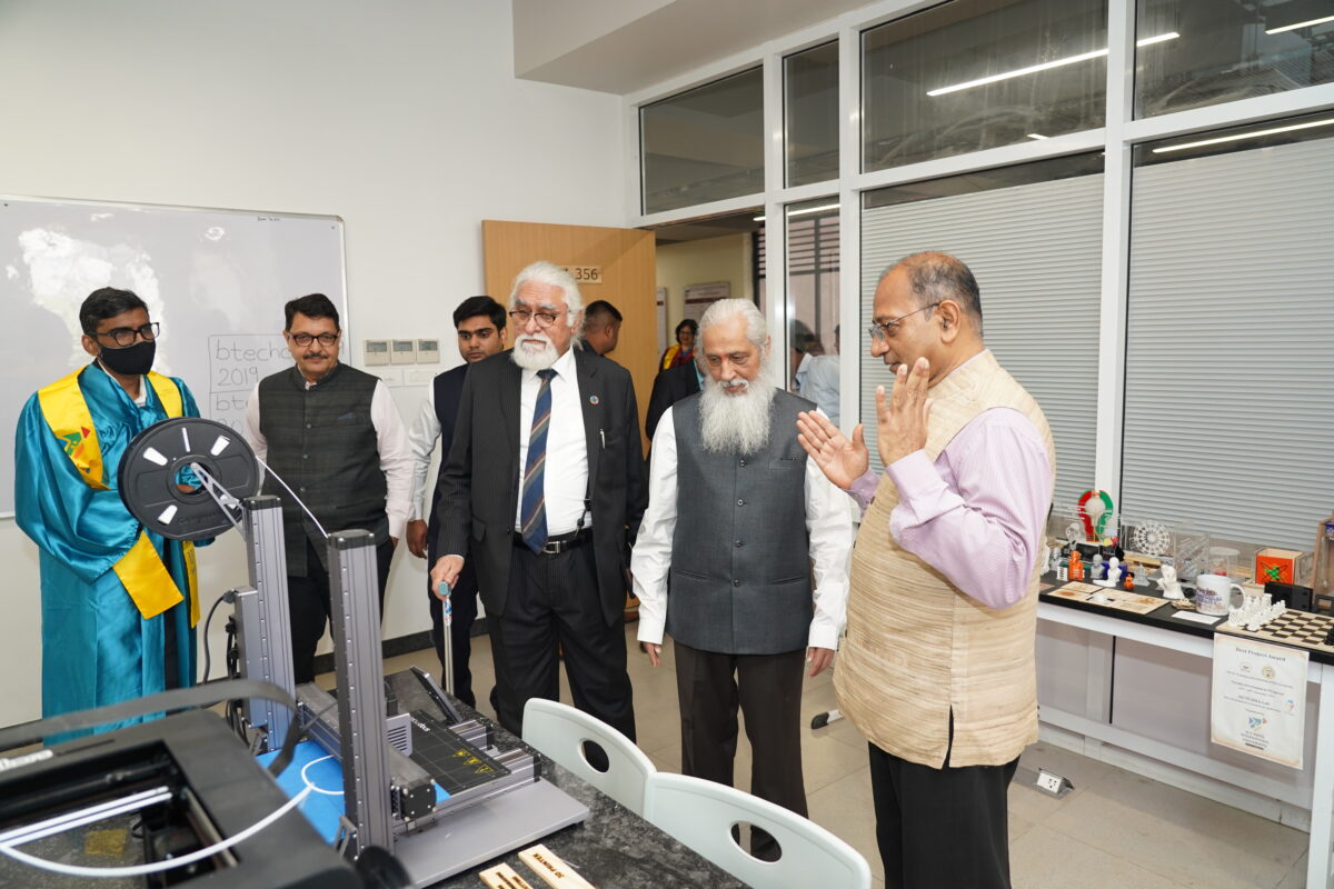
Students of DYPIU have been using our setup extensively and as classes have started to take place on the campus, its utility would continue to grow. We have a number of ongoing projects that are using these facilities. A 6 ft + humanoid robot is under development and so are projects such as “Mars Rover” etc. A group of students is also developing prosthetic limbs to provide them free of cost to the needy in nearby areas. As use is increasing, we would keep adding more of them and make it like a 3D printing farm. We would also make our own 3D printer and also procure Ceramic/Clay printer, Tissue printer, Metal printer etc.


As DYPIU setup was the newest in the series, the equipment procured by us are the most cost-effective and multifunctional option at this time. Initially, it was necessitated due to lack of space and funds but subsequently, this setup is likely to be copied across India as large numbers of IDEA Labs become functional. As the second round of institutions to benefit from this scheme goes through and with AICTE making IDEA Lab an add on to the engineering curriculum, we expect this “digital fabrication fever” to spread widely across the country. It would have a profound impact on the innovation landscape of the country and result in the growth of the manufacturing industry and GDP.